
 diglloydTools™


Reader Comment: “what Apple did with the M1 Max, it’s very impressive... Intel is really in deep trouble”
Related: Apple, Apple MacBook Pro M1, Apple Silicon, GPU, laptop, MacBook, MacBook Pro, memory, Other World Computing, reader comment, Roy P, SSD, video tech
re: Why a Desktop Computer is Often Better than a Laptop
Apple is now the state-of-the-art leader in chip design; see also: Apple rolls out the chips—M1 Pro and Max

Apple rolls out the chips—M1 Pro and Max
Apple has clearly achieved world-class semiconductor design status and has succeeded in being the first such company to get the benefits of TSMC’s 5nm process. Intel’s Pat Gelsinger acknowledged Apple’s accomplishment and has taken it as a challenge to build better chips, acknowledging that it will take time to beat Apple. The power-performance curves are an engineer’s dream and the epitome of Moore’s law.
MPG: how far can Apple scale the 5nm chip process... could we see a 16-core chip (12+4) with 128GB memory support to follow the M1 Max 10-core (8+2) chip? Such a chip would be the natural step-up for a Mac Pro or iMac 5K design.
Challenges loom for the high end: adding CPU and GPU cores and support for 128GB or more memory will chew up a lot of chip real estate. But the M1 Max chip is already huge, with 57 billion transistors. Yields quickly drop as chip area grows, but maybe that can be offset by ignoring defective GPU/CPU cores.
Reader Roy P writes:
If you see what Apple did with the M1 Max, it’s very impressive. Not only architecturally and as an SoC design, but this thing is being made at 5nm.
Intel is really in deep trouble, unless they can somehow can manage to get competitive in process technology again. AMD is the only solution available to the Windows computer makers (Dell, Lenovo, …), and AMD can copy ideas from the Apple M1, and build SoCs with X86 CPU cores + their own Radeon GPU cores. It might not be as good as the Apple designs, but it would be the next best thing, and at least, they can both put ARM cores into the same design and also go to TSMC for fab.
Intel loves ARM cores as much as it would love a growing tumor in its body as a legitimate organ. And Intel is still way behind TSMC in process technology and HVM. And if Intel decides to spin off its fabs and go to TSMC, not only will they get laughed at, but they would need to take a number and stand behind AMD for fab capacity. Pat Gelsinger has talked the talk, so it will be interesting to see if he can walk the walk.
Also interesting to see is what nVidia does. It is now harder for them to market their GPU technology – what is the outlet and who will be the customers? One scenario is nVidia buys Intel and creates a new Apple M1x competitor, with CPU + GPU + AI/ML all rolled into one, and works with Microsoft for software and OS. In that case, AMD is screwed.
Microsoft might also be worried about the huge hardware / software synergy that Apple is getting, and not be able to get that leverage, because the box makers and CPU providers are all doing their own thing. So if nVidia doesn’t make a move, it will be interesting to see if Microsoft says enough is enough, and buys out say, AMD, and create new chipset + O/S combo they can sell to the box makers like Dell and Lenovo. In that case, Intel is screwed. At least, nVidia will have enough going for it in AI/ML, automotive, etc.
We might see some tectonic plates shift in the next 2-3 years. Apple is sitting pretty. Google is another loose cannon.
Some market cap numbers to watch:
Microsoft: $2.3 T
Intel: $225 B
AMD: $141 B
nVidia: $553 B
Google: $1.9 T
Apple: $2.5 TThe brick wall Apple is likely to hit as for an M2 chip is Moore’s Law. Ten years ago, they did not have a path beyond 10 nm. The last technology node I was personally involved with was 22nm, and at that time, there was a path visible to 14 nm, and 10 nm was “may be possible”, but the universe ended there. And here we are today, in HVM at 5 nm, and there is talk about at least a 3 nm node. After that, the pace of further performance gains will almost certainly slow down quite a bit.
So I think Apple could have an M2 for sure, although at some point, it’s simply not just the raw number of cores, but also how various execution threads are or can be efficiently mapped to the cores, how the results are combined, etc. It’s the age-old problem from the MIMD (multiple input-stream, multiple data processing) days. If you could break up a task that would take a day to accomplish, and break it down to 2 billion pieces and hand a piece to every Indian and Chinese, they could accomplish the task extremely fast, but the overheads on either side of the task execution are so huge that it makes it impractical :) I’m sure you’ve heard that one before.
...
There is no upside for Apple to share the die size with anyone. Eventually, it will come out, but if Apple says nothing, that means someone will have to buy at least a minimal 14.2” MBP with M1 Max, then rip it open and blow the lid off the chip to measure it. That is probably at least a month or two away. That means another 1-2 months of FUD at companies like Intel and AMD, especially at Intel.
The M1, M1Pro and M1Max set has to be a punch in the gut for Intel and AMD, especially Intel, which is getting hit from both the design and the manufacturing fronts. So can you imagine all the calls from board members, emergency exec staff meetings, and endless speculations in the management ranks on what heads are going to roll next, etc.? If they knew the die size, they can quickly guess what kind of yields TSMC is getting, how much they are likely charging Apple, what Apple’s margins are, etc., and at least, based on that, they can formulate a plan of action. But not knowing all that for a couple of months makes it more chaotic.
Let the competition flutter in the winds for as long as possible… This is VERY impressive performance by Apple, to raise the bar so high.
Intel earnings are due tomorrow, it will be interesting to see how Pat Gelsinger responds to questions relating to Apple.
...
What that means is, the 5 nm process is truly another generation, well beyond 7 nm. Meaning, they didn’t do a typical intermediate step in migrating towards the next node, like slightly shrinking the polygons, but mainly achieving smaller transistor channel lengths by over-etching the grate Poly. That does get you smaller transistors, but the pitch at which the lines are drawn are still 14 nm or maybe 13 nm, so the overall die size does not shrink much.
With this 5 nm process, I don’t know if the pitch is really 10 nm or something more relaxed than that, like 11 or 12 nm, but it is not a 7 nm design rules (i.e., 14 nm pitch) + aggressive etch. It’s very clear that the M1 Max has a significantly larger transistor count at a considerably smaller overall die size, and that is really impressive.
Looking at the TSMC site, it’s very clear that they are very confident about a 3 nm process, and also, they are saying it will be a full node, no Mickey Mouse partial node. If that’s true, here’s very simple, quick math, no different from estimating the pixel count given a sensor size:
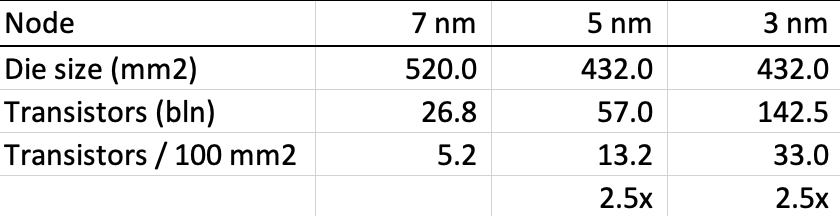 Die size vs 7nm, 5nm, 3nm process
If TSMC can maintain a node-to-node 2.5x increase in transistor count, you’re looking at a lot of cores. Even a simple doubling would still accommodate a lot more cores, on board DRAM, etc.
This is really spectacular. The saddest part of it is, such a huge part of the technology TSMC has came from UC Berkeley, including all their FINFET stuff. It has been here, languishing in the public domain, for years. Intel did not take advantage of it because of internal arrogance and incompetence, and the other semiconductor companies didn’t take advantage of it, because they could please Wall Street more by outsourcing their fabrication and test to TSMC.
MPG: Intel must be extruding bricks at this point. The TSMC “volume production” comment means that in theory, we could be looking at a 25-core CPU count, and an 80-core GPU count by mid 2022—2.5X what the Apple M1 Max chip can do. Intel would be perhaps 3 or even 5 years behind or so, most likely. Would you buy Apple or Intel stock, given that?
I’m interested more in seeing Apple take the current 10-core chip (8 performance cores + 2 efficiency cores) to more CPU and GPU cores, and support for at least 128GB memory. A 16-core would be more than ample for me for the next 4-5 years. Just going to 16 cores would blow my 28-core Intel-based 2019 Mac Pro out of the water, which is no speed demon when only a few cores are used, and runs into serious bottlenecks at a far lower clock speed when 16 or more cores are used.
The die size of the Apple M1 Max chip is a massive 432 mm^2!
According to AnandTech, the Apple M1 Max chip is a massive 432 mm^2—about 22 X 20mm. And according to
The M1 Max is truly immense – Apple disclosed the M1 Pro transistor count to be at 33.7 billion, while the M1 Max bloats that up to 57 billion transistors. AMD advertises 26.8bn transistors for the Navi 21 GPU design at 520mm² on TSMC's 7nm process; Apple here has over double the transistors at a lower die size thanks to their use of TSMC's leading-edge 5nm process. Even compared to NVIDIA's biggest 7nm chip, the 54 billion transistor server-focused GA100, the M1 Max still has the greater transistor count.
In terms of die sizes, Apple presented a slide of the M1, M1 Pro and M1 Max alongside each other, and they do seem to be 1:1 in scale. In which case, the M1 we already know to be 120mm², which would make the M1 Pro 245mm², and the M1 Max about 432mm².
